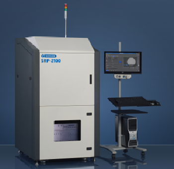
Semiconductor Wafer Level Manufacturing Equipment

Forces Driving Semi Mergers Acquisitions Ee Times Semiconductor Semiconductors Merger

Inspecting Unpatterned Wafers

Semiconductor

Advantest M6761ad Dynamic Test Handler For Sale Jmc Worldwide Semiconductor Equipment Semiconductor Semiconductor Manufacturing Test

Fine Tuning Chemical Mechanical Polishing Head With Fuji Prescale Film Keywords Wafer Polishing Semiconductor Production Cmp Semiconductor Mechanic Repair
Semiconductor Wafer Metrology Tools Compare Review Quote Buy

Wafer level packaging wlp is becoming an important semiconductor packaging technology.
Semiconductor wafer level manufacturing equipment.

Silicon Wafers Producers And Suppliers Company Semiconductor Materials Low Stress Semiconductor

Semiconductor Wafer Processing Ic Packaging Testing Solutions Leica Microsystems

Semiconductor Wafer Cleaning Equipment Market Report Ability
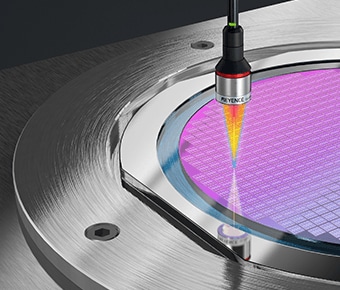
Semiconductor Wafer And Glass Substrates Inspection Inspection Methods For Quality Assurance Coating Dispensing Technology Keyence America
Source : pinterest.com
